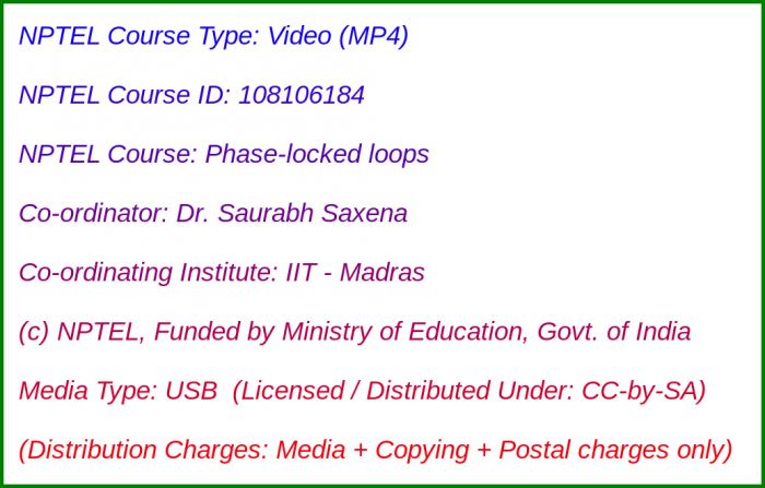
Media Storage Type : 32 GB USB Stick
NPTEL Subject Matter Expert : Dr. Saurabh Saxena
NPTEL Co-ordinating Institute : IIT Madras
NPTEL Lecture Count : 65
NPTEL Course Size : 6.9 GB
NPTEL PDF Text Transcription : Available and Included
NPTEL Subtitle Transcription : Available and Included (SRT)
Lecture Titles:
Lecture 1 - Course Introduction and Motivation - Part I
Lecture 2 - Course Introduction and Motivation - Part II
Lecture 3 - Basic Operation of a Phase Locked Loop
Lecture 4 - Simple Implementation of a Phase Locked Loop
Lecture 5 - Input Output Characteristics of Basic PLL Blocks
Lecture 6 - Time Domain Analysis of a Simple PLL
Lecture 7 - Time Domain Versus Small Signal Analysis of a Simple PLL
Lecture 8 - Type and Order of PLL
Lecture 9 - Small Signal Analysis of Type-I/II/III PLLs for Phase Step, Frequency Step and Frequency Ramp
Lecture 10 - Frequency Acquisition Range for PLLs
Lecture 11 - Frequency Acquisition in Type-I PLLs
Lecture 12 - Frequency Acquisition Limits in Type-I PLLs
Lecture 13 - Frequency Acquisition in Type II PLLs
Lecture 14 - Frequency Acquisition Ranges in Type II PLLs with Ideal and Non Ideal Integrator
Lecture 15 - Frequency Domain Insight in Frequency Acquisition for Type II PLLs
Lecture 16 - Introduction to Clock Multipliers
Lecture 17 - Analog Phase Error Detectors - Part I
Lecture 18 - Analog Phase Error Detectors - Part II
Lecture 19 - Digital Phase Error Detectors - Part I
Lecture 20 - Digital Phase Error Detectors - Part II
Lecture 21 - Range Extension for Phase Error Detectors
Lecture 22 - Phase Frequency Detector
Lecture 23 - Digital Frequency Detector
Lecture 24 - Charge Pump PLL
Lecture 25 - Small Signal and Stability Analysis of Type II Order 2 Charge Pump PLL
Lecture 26 - Problems in Charge Pump PLL - Dead Zone in PFD
Lecture 27 - Problems in Charge Pump PLL - Reference Spur
Lecture 28 - Design Procedure for Type-II Order 3 Charge Pump PLL
Lecture 29 - Design Procedure for Charge Pump Clock Multiplier
Lecture 30 - Sources of Non-Linearities in CP-PLL - Part I
Lecture 31 - Sources of Non-Linearities in CP-PLL - Part II
Lecture 32 - Noise Analysis in CP-PLL - Part I
Lecture 33 - Noise Analysis in CP PLL - Part II
Lecture 34 - Noise Analysis in CP-PLL - Part III
Lecture 35 - Noise Simulations for CP-PLL Blocks
Lecture 36 - Introduction to Oscillators
Lecture 37 - Low Swing Ring Oscillator - Part I
Lecture 38 - Low-Swing Ring Oscillator - Part II
Lecture 39 - Large-Swing Ring Oscillator - Part I
Lecture 40 - Large-Swing Ring Oscillator - Part II
Lecture 41 - Large-Swing Ring Oscillator - Part III
Lecture 42 - Large-Swing Ring Oscillator - Part IV
Lecture 43 - Large-Swing Ring Oscillator - Part V
Lecture 44 - Supply Regulated VCO - Part I
Lecture 45 - Supply Regulated VCO - Part II
Lecture 46 - Supply Regulated VCO - Part III
Lecture 47 - Phase Noise in Ring Oscillators
Lecture 48 - Circuit level Design of PFD - Part I
Lecture 49 - Circuit level Design of PFD - Part II
Lecture 50 - Circuit level Design of PFD - Part III
Lecture 51 - Circuit level Design of Charge Pump - Part I
Lecture 52 - Circuit-level Design of Charge Pump - Part II
Lecture 53 - Circuit-level Design of Charge Pump - Part III
Lecture 54 - Circuit-level Design of Charge Pump - Part IV
Lecture 55 - Circuit-level Design of Charge Pump - Part V
Lecture 56 - Circuit-level Design of Charge Pump - Part VI
Lecture 57 - Circuit-level Design of Clock Frequency Divider
Lecture 58 - Techniques for Wide Frequency Range Clock Multiplier
Lecture 59 - Introduction to Digital PLL
Lecture 60 - Design of Time-to-Digital Converter
Lecture 61 - Small Signal Analysis of Digital PLL
Lecture 62 - Noise Analysis in Digital PLL
Lecture 63 - Analog/Digital Hybrid PLL - Part I
Lecture 64 - Analog/Digital Hybrid PLL - Part II
Lecture 65 - Course Summary

